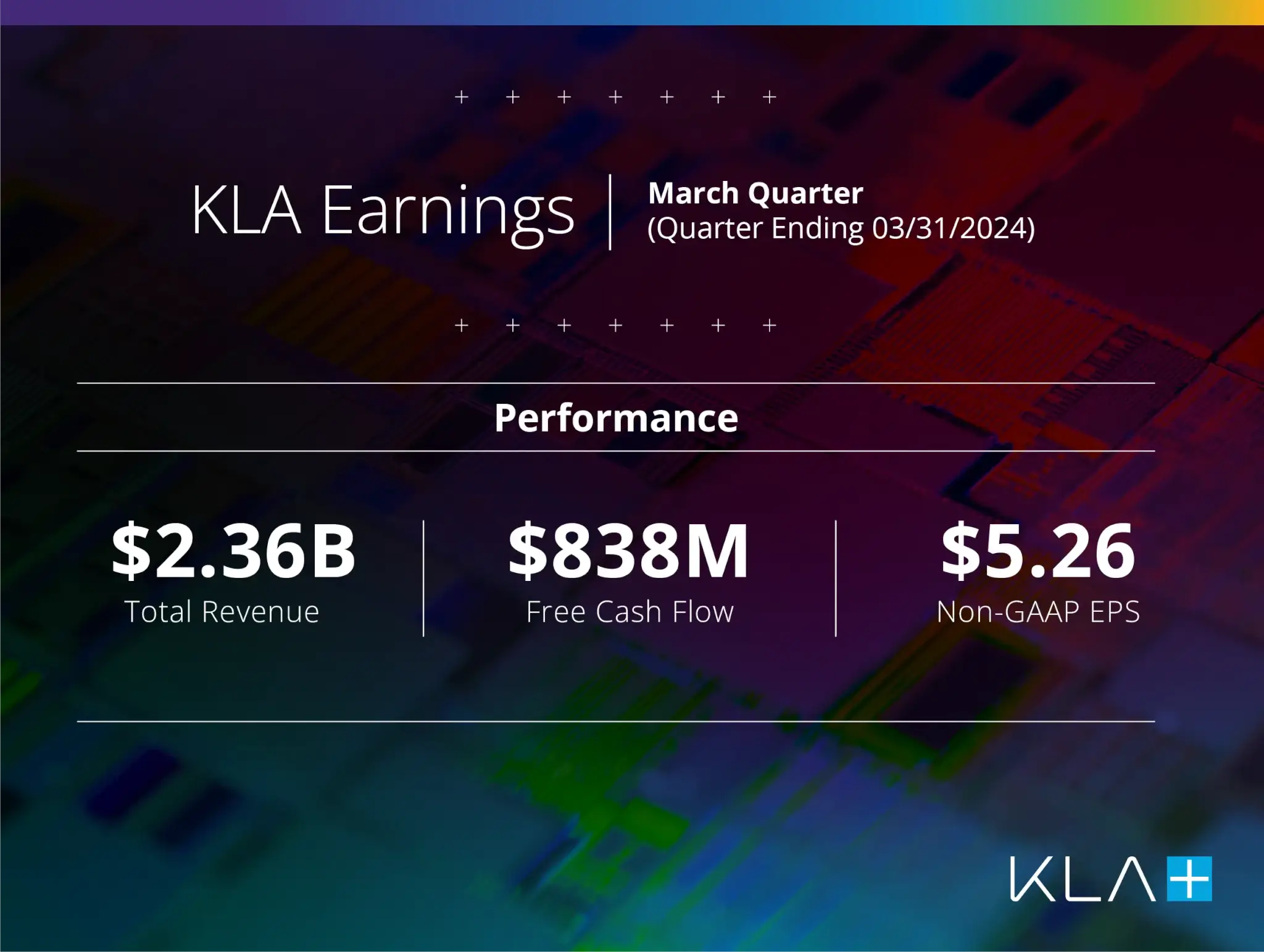
Return to KLA Advance

Leadership

Q&A: KLA’s John Robinson Reflects on 2024 SPIE Conference

Mar 1, 2024 3 min read

We sat down with John Robinson, Ph.D., senior principal scientist at KLA and SPIE fellow, for some thoughts on the 2024 SPIE Advanced Lithography + Patterning Symposium and his long involvement with the event.

This year I am the co-chair of the SPIE Advanced Lithography + Patterning Symposium, which includes six technical conferences. In this role I help with organization and operations of the symposium and set the strategic direction for the symposium’s future. Additionally, I’m on the Program Committee for the Metrology, Inspection and Process Control Conference, one of the six conferences in the Advanced Lithography + Patterning Symposium. The Program Committee sets the conference agenda, reviews papers and chairs conference sessions. One of the highlights for me is acting as the liaison for the Karel Urbánek Best Student Paper Award, which is sponsored by KLA.  

John Robinson is senior principal scientist at KLA.
John Robinson, Ph.D., is senior principal scientist at KLA. Read more about him.
KLA had a major presence at the 2024 SPIE Advanced Lithography + Patterning Symposium.

The future of EUV lithography is one of the key topics of the SPIE Advanced Lithography + Patterning Symposium 2024. For example, Ann Kelleher, executive vice president and general manager of technology development at Intel Corporation, gave a plenary presentation entitled “Evolution of advanced lithography and patterning in the system technology co-optimization era of Moore’s law.” By 2030 the semiconductor industry is expected to become a $1 trillion industry, with leading-edge chips utilizing new transistor architectures, backside power delivery and 3D chip packaging – all while approaching angstrom-level design nodes due to processing innovations, such as high-NA EUV lithography.  

Bringing together the best minds of industry, academia and government laboratories to discuss the latest challenges and solutions is one of the best ways to accelerate progress. Often new “pie in the sky” ideas originate in discussions at SPIE Advanced Lithography + Patterning, and in the years that follow they become research topics and then finally get reported as successful high-volume manufacturing methods. Examples include immersion lithography, multi-patterning and EUV lithography.

While it is clear that strict Moore’s Law “Dennard scaling” is no longer in play, scaling continues, as do innovations on multiple levels. Driven by the increasing demands of AI, transistor scaling is only part of the equation. Advanced packaging is becoming a larger part of the improved performance puzzle. In addition, there are many “More than Moore” opportunities such as wafer-based optics, sensors, photonics and the like.

According to one of the symposium’s plenary speakers, Todd Younkin, president and CEO of The Semiconductor Research Corporation (SRC), the average age of semiconductor R&D personnel is 57 years, highlighting a key need for fresh talent. For over 10 years, KLA has sponsored The Karel Urbánek Best Student Paper Award, which recognizes the most promising contribution to the field by a student, based on the technical merit and persuasiveness of their paper presentation at the SPIE Metrology, Inspection and Process Control Conference. Named after Tencor Instrument’s founder, and sponsored by KLA’s Semiconductor Software Solutions Division (MACH), it provides recognition for student contributions to the industry. Often, the student presentations are on par with those of seasoned professionals, and their contributions continue as many of them continue on as employees at KLA or other peer companies.

KLA's John Robinson presents Karel Urbánek Best Student Paper Award at the 2024 SPIE Advanced Lithography + Patterning Symposium.
John Robinson (center) presents the 11th Karel Urbánek Best Student Paper Award to Tao Shen (holding award).

Subscribe to receive
News from KLA

Blog Subscribe
Data Transfer *
Marketing *

Are you sure?

You've selected to view this site translated by Google Translate.
KLA China has the same content with improved translations.

Would you like to visit KLA China instead?


您已选择查看由Google翻译翻译的此网站。
KLA中国的内容与英文网站相同并改进了翻译。

你想访问KLA中国吗?

If you are a current KLA Employee, please apply through the KLA Intranet on My Access.

Exit